Digital Filter System

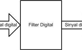
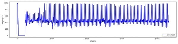
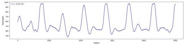
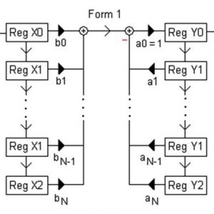
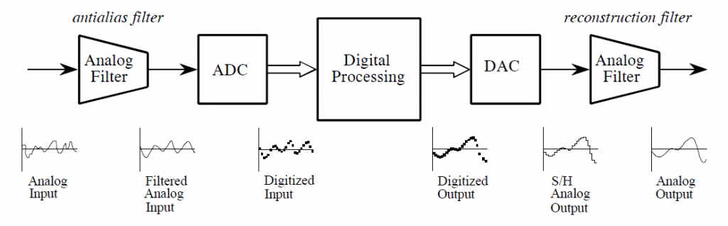
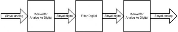
A digital filter system in principle has a diagram block as follows:

Digital filter System

In practice, the system needs some additional details in order to be implemented with a microprocessor or digital system (e.g. FPGAS).

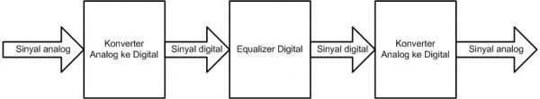
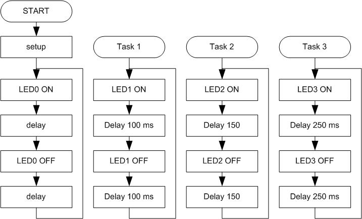
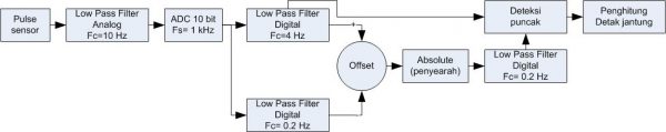
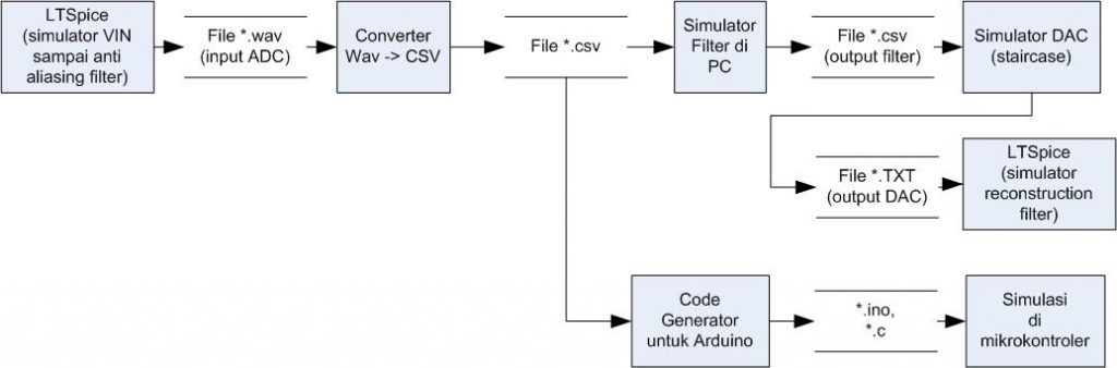
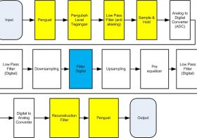
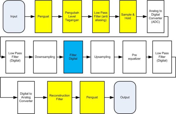
Here is a complete system of digital filters to implement with the microprocessor system:

Digital filter System Details version 1

Explanation

  • Input: input signal derived from input, e.g. for audio system can be microphone, or MP3 player, or computer.
  • This input signal has a certain level of voltage and impedance. Often these signals need to be strengthened first. E.g. microphones usually have a strong signal of tens to hundreds of millivolts with a hundreds of ohm impedance.
  • Amplifier: Amplifier has buffering function and also adjusts the amplitude to match the amplitude of used ADC.
  • Voltage Level changer: the input voltage in the form of alternating voltage, can have positive and negative voltage. The ADC used can often only accept positive voltages, so the input voltage must be shifted to be positive.
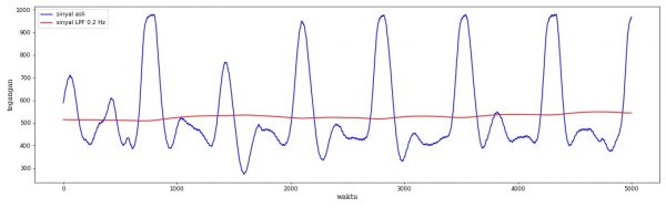
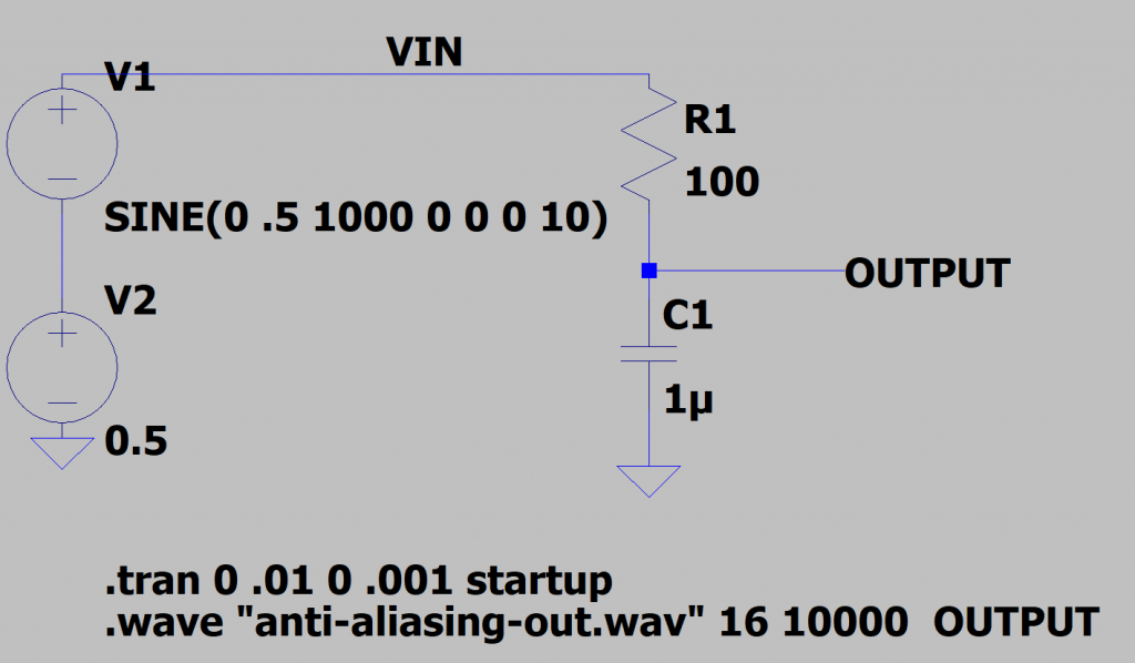
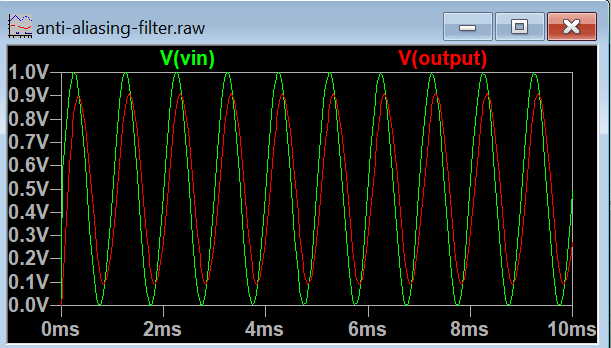
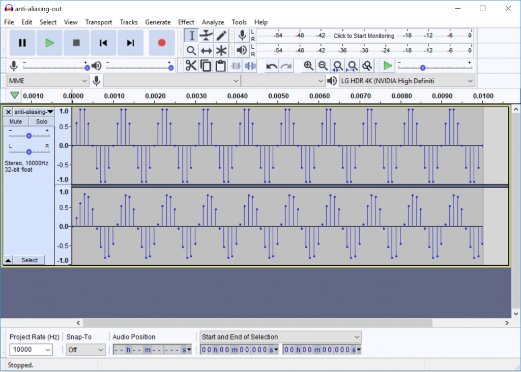
  • Low Pass Filter (anti aliasing): According to signal theory, the sampling frequency has at least 2x the frequency of the signal working frequency measured. The input signal more than 1/2 sampling frequency must be filtered so as not to happen aliasing.
  • ADC (Analog to Digital Converter): Converts the Analog voltage into a Digital number, with a certain bit resolution, and a specific sampling rate.
  • Digital Filter: Perform the desired signal processing process, can be LPF (Low pass filter), HPF (High pass filter), BPF (band pass Filter), BSF (band stop Filter) or Equalizer.
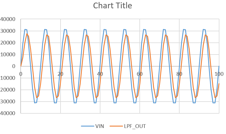
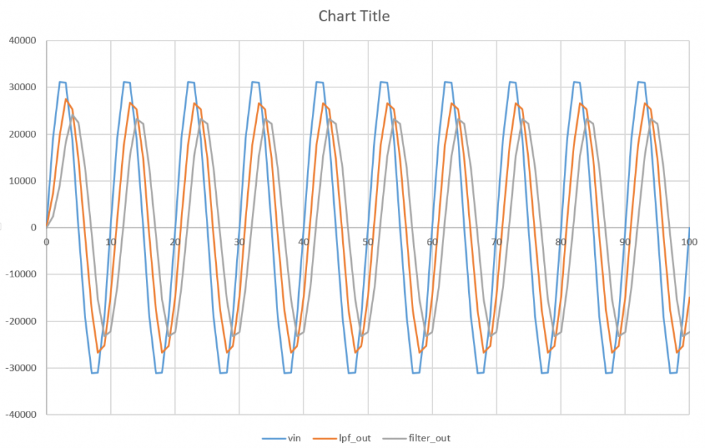
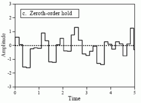
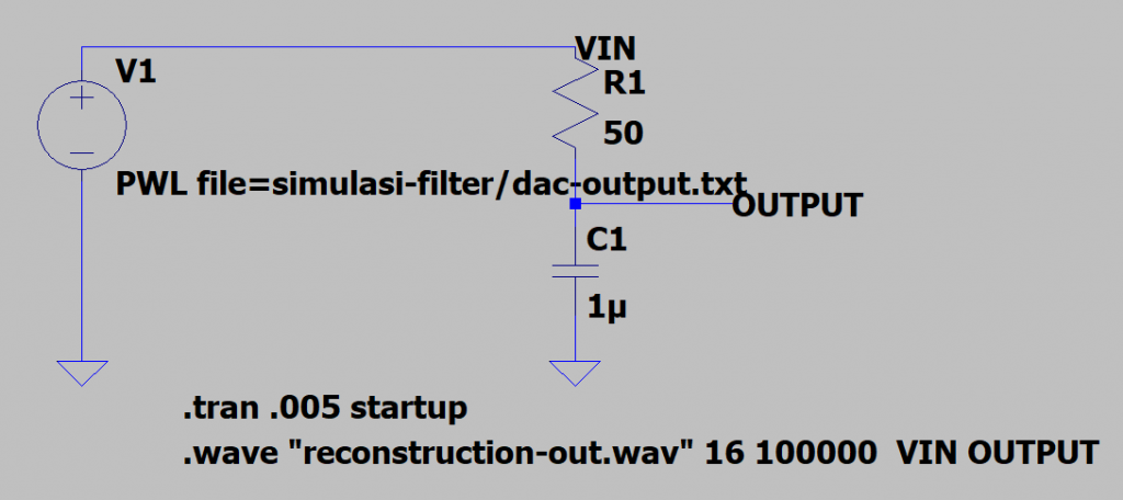
  • Digital to Analog Converter: Converts the digital signal into an Analog signal. It generally uses the principle of ZoH (Zero order Hold).
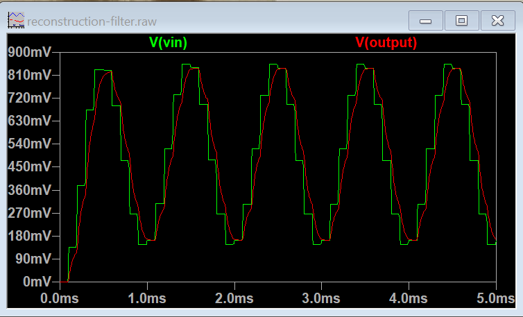
  • Reconstruction Filter: The signal from Zero order Hold has a ladder-like staircase, so it has a high frequency component. Therefore, there needs to be a reconstruction filter that removes the high-frequency component. In addition, ZoH also changes the frequency response, giving attenuation at high frequencies. Ideally reconstruction filter also compensates for it.
  • Amplifier: To adjust the voltage and impedance level from the DAC to the next stage
  • Power supply: Implicit all electronics systems need power supply. Digital processing systems have analog and digital parts, so they need to have their own voltage and power supply level.

The above system is already working well, but it has some disadvantages:

First issue: Conversion of analog to digital

  • Anti aliasing filter is difficult to create ‘ sharp ‘, so the sampling frequency must be much higher than the signal working frequency. If the sampling frequency is too close, the working frequency response is affected by an anti aliasing filter, or also some high frequency signal may penetrate the anti-aliasing filter.
  • Due to the high sampling frequency, the digital filter section must work at a higher frequency than the signal working frequency.
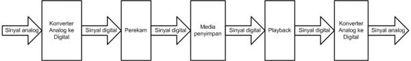
  • It also affects if the signal needs to be stored: storage will grow
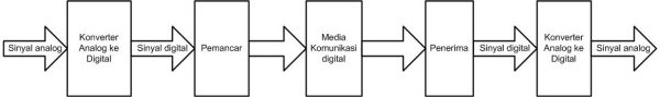
  • It also affects if the signal needs to be sent: communication bandwidth needs to grow.
  • Solution: Sampling is performed with a high frequency, but the sampling frequency is lowered (downsampling) before the signal is processed/shipped/stored.
  • In the downsampling process, the signal needs to be filtered digitally so that it does not occur aliasing. Digital filter process is easier than analog filter, especially due to the accuracy problem of analog component value.

Second issue: Digital conversion to analog

Zero order Hold on the DAC has a frequency response sinc (), so there is attenuation at high frequencies

  • Solution 1: The digital signal is changed to a high frequency before going into the DAC, thus the influence of high-frequency attenuation decreases.
  • Solution 2: The digital signal is reinforced first at high frequencies with the equalizer, in order to compensate for attenuation in high frequencies.

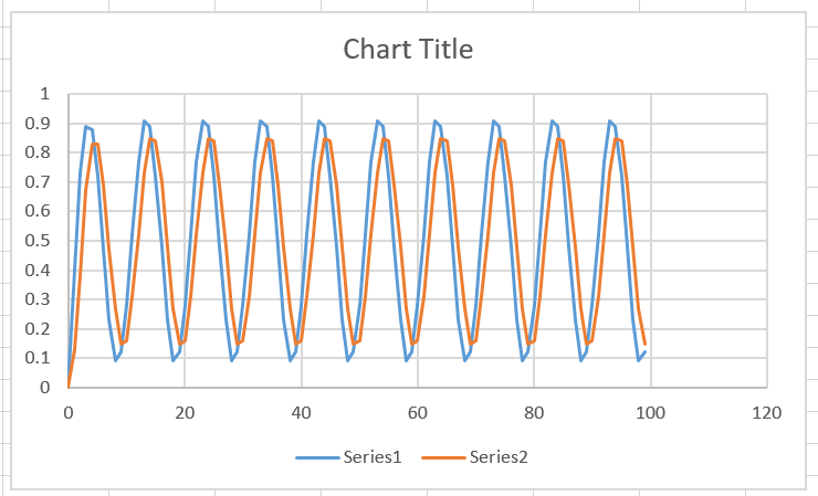
Here is the process of signal equalization to compensate for the effect of ZoH.

Equalizing
Equalization of digital signal to analog

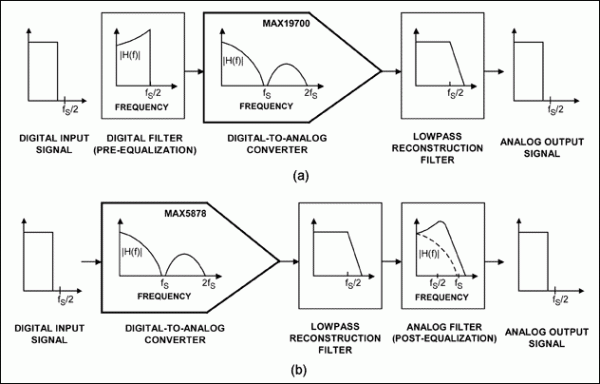
In the solution (a) The equalization process is performed digitally before the DAC, referred to as the pre-equalization stage.

In the solution (b) The equalization process is performed analogous after the LPF, referred to as the post-equalization stage.

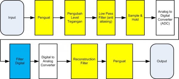
Here is a diagram block of digital filter system with these solutions:

Complete Digital filter System version 2

In this system was selected pre-equalization digitally, with consideration of designing the equalizer digitally easier. The process of creating this equalizer can be done by the ‘ Design of FIR Filters Using the Frequency Sampling method ‘ method.


Reference

Electronic system with Analog signal and Digital signal

An analog signal can be converted into digital and vice versa. This technique has several benefits. In this paper only discussed examples of applications that are LTI (Linear Time Invariant).

Here are examples of some systems in which there are analog signals and digital signals:

  • Digital filters
  • Digital Equalizer
  • Digital recorders
  • Digital communications

Theories to Master:

  • Analog Circuit
    • Analog Filter (LPF, HPF)
    • Circuit amplifier (pensum, amplifier)
    • DC power supply, including the regulator
  • Interfacing & Microprocessors
    • Microprocessor Programming with C language
    • Analog input on the microprocessor
    • Analog output on the microprocessor
    • ADC (Analog to Digital Converter)
    • DAC (Digital to Analog Converter_
    • Interruptions in microprocessors
    • Quantization error on ADC/DAC
  • Digital Signal Processing:
    • Analog/Digital Equalizer
    • Design based on the frequency response
    • Multirate on PSD
    • Digital Filters (LPF, HPF, BPF, BSF)
    • Oversampling on digital signal processing
    • Undersampling/decimation on the digital signal processing

Digital Filter

Digital filter System

In this system, the analogue signal was changed into digital, so that the process of filtering (Tapisan) digitally. After that the signal is returned to analog signal.

Common Types of Potion:

  • LPF: Low pass filter
  • HPF: High pass filter
  • BPF: Band pass Filter
  • BSF: Band Stop Filter

The filter can be done in the analog domain, but in some cases there are excess on digital filters, so it is better if the filter process is performed in the digital domain.

Digital Equalizer

Digital Equalizer System

In this system the analog signal was changed first to digital, to be done the equalization process digitally. After that the signal is returned to analog signal.

The equalization process is the process of changing the frequency composition on a signal (Wikipedia)

Digital Recorder

Digital Recorder System

In this system the analogue signal was changed first to digital, to be then stored in a media. After that the saved signal can be read and issued at another time. After that the signal is returned to analog signal.

Digital Communication System

Digital communication System

In this system the analogue signal was changed first to digital, to be then sent by the transmitter through a communication media. In the receiver the signal is changed again into a digital signal.. After that the signal is returned to analog signal.

Digital communication has some advantages over analog communication.

Analysis of Power Supply Circuit

Problems:

Want to raft amps using a CT 18 VAC transformer But after passing the Spull diode so 34 VDC


The circuit is a full-wave bridge rectifier, with the following schemes (source):

The signal form of the above series is still not flat, because there are no filter capacitors yet.

The input voltage takes from the terminal 18 volts and 18, while the transformer has a tap center (CT), so the AC voltage that goes into the bridge diode is 18 volt RMS (root mean square).

To illustrate this signal, it needs to be converted to peak voltage, with the formula Vpeak = Vrms * 1,414, so Vpeak = 36 x 1,414 = 50,904 Volt

The bridge output voltage form is as follows (green color signal), compared with the input signal (red color):

Actually, the bridge output signal will be reduced slightly as there is a drop voltage on the diode, but in that image the drop voltage is ignored first.

If the bridge output voltage is measured by DC voltmeters, then the measured voltage is the average of the green color. The formula is Vaverage = 0637 Vmax = 0.9 Vrms

SOURCE rumurs: https://www.electronics-tutorials.ws/power/single-phase-rectification.html

The diagram as follows:

The green signal is the output of the bridge, the synusoidal signal that has already been seared.

The measured voltage at the DC voltmeter is the average of 32.4 volts

In measured photos is 34.6 volts, likely due to imprecision of the output voltage of the transformer. If you want more definite, it can be measured how much the output voltage of the transformer or bridge inputs with the AC voltmeter (AVOmeter on the AC setting).

Tip: The standard AVOmeter on the DC setting is only designed to measure DC or average voltage, while in the AC setting only for measuring AC rms voltage (root-mean-square). If the form of the signal is not a DC or pure AC, then the displayed number is less precise. On a signal that is not DC or AC is pure, it is more appropriate to use an oscilloscope to measure the signal.

Bird Sounds with Arduino

Here is an example of a bird’s voice generation using the Arduino Nano microcontroller (ATmega328)

The code is taken from http://120.107.171.121/~tywua/sub/ISAR/Chirp.ino, apparently from a professor’s website at National Changhua University of Education, Taiwan.

Arduino Bird Sound Generation

Here is an example of the resulting sound:

Here’s the signal form in the Audacity app for 1 set of tweets only:

Here’s the source code (from http://120.107.171.121/~tywua/sub/ISAR/Chirp.ino)

int piezopin = 11;  Select the PIN for the speaker
int angulo = 0;
int counter = 0;


void Setup () {
  pinMode (Piezopin, OUTPUT);
}
void Loop () {
  Angulo = random (10.50);
  Counter = random (2.6);

  highChirp (5, Angulo/10);
  Delay (100);
  lowChirp (Angulo * 4.2);
  Delay (100);
  Tweets (counter, 2);
}

void highChirp (int intensity, int chirpsNumber) {
  I.
  int x;
  for (int veces = 0; veces<=chirpsNumber; veces++){
    for (i = 100; i > 0; I--)
    {
      for (x = 0; x<intensity;  x++)
      {
        digitalWrite (Piezopin, HIGH);
        delayMicroseconds (i);
        digitalWrite (Piezopin, LOW);
        delayMicroseconds (i);
      }
    }
  }
}

void lowChirp (int intensity, int chirpsNumber) {
  I.
  int x;
  for (int veces = 0; veces<=chirpsNumber; veces++){
    for (i = 0; i<200; i++)
    {
      digitalWrite (Piezopin, HIGH);
      delayMicroseconds (i);
      digitalWrite (Piezopin, LOW);
      delayMicroseconds (i);
    } 
    for (i = 90; i > 80; I--)
    {
      for (x = 0; x<5;  x++)
      {
        digitalWrite (Piezopin, HIGH);
        delayMicroseconds (i);
        digitalWrite (Piezopin, LOW);
        delayMicroseconds (i);
      }
    }
  }
}

VOID tweet (int intensity, int chirpsNumber) {

I.
int x;
Normal chirpsNumber 3, normal intensity 5

for (int veces = 0; veces<chirpsNumber; veces++){
  for (int i = 80; i > 0; I--)
  {
   for (int x = 0; x<intensity;  x++)
   {
     digitalWrite (Piezopin, HIGH);
     delayMicroseconds (i);
     digitalWrite (Piezopin, LOW);
     delayMicroseconds (i);
   }
  }
}
Delay (1000);
}


Blinking LED on Arduino With Interrupt and RTOS

Making flashing LEDS is one of the simplest ways to demonstrate the timing capability of microprocessors.

Here are some techniques you can do:

  • Timer interruptions
  • Standard Arduino delay
  • Delay from FreeRTOS

Standard Arduino Delay

Delay on Arduino explained at https://www.arduino.cc/reference/en/language/functions/time/delay/

On standard Arduino software such as Arduino Nano and UNO, this delay is implemented with the Loop software.

Example of a software using this delay is an example of Blink software on Arduino (https://www.arduino.cc/en/tutorial/blink)

The flow Diagram of the Blink program is as follows

Flow Diagram of Blink ()

A Delay on FreeRTOS

FreeRTOS allows the Arduino software to have multiple loops at the same time.

Ported FreeRTOS for Arduino UNO and Nano can be viewed at https://github.com/feilipu/Arduino_FreeRTOS_Library

This FreeRTOS Library can be installed on the Arduino IDE from the Tools-> Manage Libraries menu. Then search by keyword FreeRTOS.

The FreeRTOS library installation process

For example, here is a flowchart diagram of a program that makes the LEDS blink with 3 loops. Each LED has a different frequency.

Flashing with FreeRTOS

The Source code can be viewed at https://github.com/waskita/embedded/tree/master/atmega-blink-freertos

The FreeRTOS function used is

Arduino with LED flashing

Here’s the Arduino Nano hardware demo

Timer Interruptions

Under construction

Dehumidifier on the Wonderful Dry Cabinet

Generally, House painters in GA can help you out in cabinet painting .But what is meant by dry cabinet ? Dry cabinet is useful for storing objects that must be stored at low humidity. For example camera and camera lens. Besides Dry cabinet, you can also use dry box. The main difference: the dry cabinet uses an auto-powered dryer (dehumidifier), while the dry box must be dried with a dryer that must be replaced/regenerated if already saturated.

Here are the stages of fixing a dehumidifier on the Wonderful AD-068C dry cabinet. Short story There is a cable that broke in it, so the drying process does not work.

Here’s a look ahead of the Wonderful dry box.

Wonderful dry Box Dehumidifier Front

Here is a drying device located at the back of the dry cabinet box.

Wonderful dry box dehumidifier backside container

This dryer can be uninstalled by removing the first 4 screws in 4 corners.

The following appears behind the dryer that was removed from the box.

Wonderful dry box dehumidifier back box

Here is the front view of the dryer. There appears to be moisture-regulating knop. This Knop function is to adjust the moisture you want to achieve in the dry box box. There are no moisture figures on the knop, so the moisture adjustment is more by trial-and-error.

Wonderful dry box dehumidifier front Box

Here’s the inside of the dryer box.

Wonderful dry Box Dehumidifier controller and heater
The inside of the Dryer box (Part 1)

Here’s the inside of the front that contains the moisture regulator.


Wonderful dry Box Dehumidifier Moisture Controller
The inside of the Dryer box (Part 2)

After checking it turns out there is a cable disconnect. The cable is a spring heater that moves the valve.

After the problem was discovered, the cable was died by soldered. Goes wrong.

How this dryer box works is interesting. Approximately as follows:

  • Moisture sensors detect moisture in the dry cabinet box. If humidity is less than a certain threshold, then there is a switch that becomes ON. If humidity is low enough, the switch becomes OFF.
  • The main component of the dryer is using the granules I suspect are silica-gel. Silica gel can absorb water in the air, so the air becomes dry. But there is a limit, so if it is saturated then silica gel is not able to absorb water anymore.
  • Silica gel is dried by heated way with electric heater. This heater is controlled by a controller.
  • There is a valve that regulates whether silica-gel is connected to the dry cabinet, or is connected to the outside of the dry cabinet.
  • When it is drying, silica gel must be connected to the dry cabinet so as to absorb moisture in the dry cabinet.
  • When silica-gel is heated, silica gel must be connected to the outside of the dry cabinet, so that steam released water does not go into the dry cabinet.
  • There is a valve whose function connects silica gel to the outside or into the inside. The valve is driven by a spring. Uniquely, the spring shrinks if it is heated, and relaxs if cooled. I guess this spring uses metal-recall-shape (Shape-memory-alloy).
  • There are 2 heaters on this system, the first function of drying silica-gel, the second the function of moving the valve spring.
Wonderful-dry-cabinet-spring drawn valve
Valves when pulled by a spring
Wonderful-dry-cabinet-saggy valve
Valve with loose spring

Heart Rate Signal Analysis

In this article outlined analysis of heart rate signals. A heart rate signal is obtained from the pulsesensor sensor.

This Sensor has been discussed in some of the previous articles:

The addition of this article is a filtering with LPF to help smooth the signal of the sensor results.


Heart rate Sensor from pulsesensor.com

The signal processing stage is as follows:

  • Pulsesensor as a source of signal coming from the heartbeat
  • The voltage signal from the sensor is inserted into the resistor Filter and the capacitor as a low pass filter to avoid aliasing,
  • The filter result voltage is inserted into the Arduino Nano module to be converted to digital with ADC. Data sampled with 1 kHz frequency with ADC on the Arduino Nano,
  • Digital Data is then transmitted by asynchronous serial communication at a speed of 115200 bps through the USB port to the PC desktop.
  • Data recorded on desktop PC with RealTerm software. Data is recorded to a TXT file on the PC.
  • Record result Data is then analyzed with Python software using Jupyter Notebook

The software for the data measurements on the Arduino is as follows: https://github.com/waskita/embedded/tree/master/atmega-detak-jantung-profiling

The software for the analysis of signals is as follows: https://github.com/waskita/embedded/blob/master/analisis-detak-jantung/heart-beat-analysis-1kHz.ipynb

Here’s a signal flow block diagram on this system:

Here is details of the signal flow description of the system

Signals of measurement results from ADC
The original signal is enlarged

The purpose of the sensor is to measure one’s heart rate.

There are a few things that complicate heart rate calculations:

  • The amplitude of the signal varies depending on the hand condition, pressure on the sensor, and so on, so the signal threshold
  • The heart rate signal has a high peak, and there are also smaller peaks. There must be an algorithm to detect high peaks only.

The ADC signal measurement results are still less flat, so to make the smoother filtering carried out at a frequency cut off of 4 Hz. The cut-off frequency of 4 Hz is selected considering the maximum heart rate of a normal person is 220 per minute, or equivalent to 3.667 Hz. So the signal above the frequency 3.667 Hz is not required. 

Filter using a digital filter of IIR 4 pole. The 6 pole filter produces an unstable filter, and finally 4 pole is used. IIR filter types so that calculations are simpler, since this system will be implemented on microcontrollers with limited computing capabilities.

Design filter using Iowa Hills IIR Filter Designer Version 6.5 as follows:

Implementation of filters with Python language, using the filter structure “Nth Order Coeffiecients”.

The structure of the IIR (Infinite Impulse Response) filter used is as follows:

The filter result is as follows (red signal).

Filter result signal with low pass with FC = 4 Hz

The measurement Hasi signal contains a DC signal offset, so the average is not 0. To eliminate the DC offset, is done filtering with LPF at 200 mHz. Filter 2 pole IIR.

The filter results are as follows (red signal):

LPF 0.2 Hz Signal Filter result

Signal without offset is obtained with the filter result signal 4 Hz reduced by the filter result signal at 0.2 Hz.  The result is a signal (blue color) in the image below.

The blue signal is then seared (rectified), so there is a red signal.

Offset signal results and directives


The redirect signal is filtered again with the 0.2 Hz filter, to help peak detection. Peak detection is somewhat difficult, because of the 4 Hz filter results There is still a small peak. With the signal of a referral result is expected to detect high peaks only.

Signal Combination

The final process is peak detection. Only high peaks are counted.

Pulse top detection of heart rate

Cover

From experiments made, analog and digital filtering can help shape the signal so that it is easier to process.

Reference

Using Bigger Power Supply Than Necessary

Electronic devices require a power source, one of which is an adapter. The need for electrical devices is usually expressed in voltage and current, e.g. 12 volts, 5 amperes. One of the most confusing problems is what if the adapters available for the voltage match, but the ones are bigger than necessary.


Issues

Examples of the issue are as follows:

Sorry to ask about the adapter.
Is the adapter 12 volt 5 Ampere (Think of pure 5 ampere), it means he took out the voltage 12 Volt and 5 Ampere constant cur
rent? Or flows that are issued only fit the load that is passed?
For example, the load is 12 volt 1A, if the adapter is 12 Volt 5 A, then The adapter outputs only 12 volt 1A to fit its load?

Or instead, the lights can be damaged due to the output of the full 5 Ampere adapter.

Answer

A widely sold adapter can generally be viewed as a voltage source. This means the adapter maintains constant voltage, while current changes as needed. The adapter has a maximum current limit, above the limit that the voltage cannot be guarded (down) or the fuse is broken.

So the use of an adapter that is very much bigger than necessary is not a problem. The Adaptor will provide the voltage as stated (e.g. 12 volts), while the supplied current will be adjusted to the current required by the electronic device. Usually the required current will vary depending on what the device is working on.

Controlling DC Motor with Microcontroller

PID without PhD Cover

Here’s a quick article to create a digital controller without too many theories: “PID without PhD” 

The article writes a fairly complete digital handbook, discussing from digital control theory to source code, minus Rotary Encoder & PWM. Tim Wescott, Applied Control Theory for Embedded Systems, Newnes 2006

Some problems:


Yesterday I had tinkering a few hours, the summary as follows. Some things that might make the problem:

1. Specifications Rotary Encoder, able to how many rpm?

2. Interfacing encoder into a microprocessor. Is the signal from the encoder well received in the microprocessor?

3. External interrupt settings, is it correct?

4. Time to interrupt: Does the CPU quite quickly process the data before the next interrupt comes? Is lower interruptions a priority CPU allowance?

5. Is there any other process in the microprocessor that rebutted the CPU ration?


Use of interruptions in STM32:

https://circuitdigest.com/microcontroller-projects/getting-started-with-stm32-development-board-stm32f103c8-using-arduino-ide
https://circuitdigest.com/microcontroller-projects/how-to-use-interrupts-in-stm32f103c8


Alternative Motor Driver

Alternative Motor drivers:

– TB6612FNG

– L293

– L298

-Discrete MOSFET

-Discrete BJT


DigitalWrite Slow

https://www.peterbeard.co/blog/post/why-is-arduino-digitalwrite-so-slow/


Reference

Digital Signal Processing Simulation

Simulation stages of digital signal processing with LTSpice, and compiler C

This document focuses on showing the occurrence of processes at each stage and integration of those processes, not discussing system optimization or subsystem.

Preparation

  • Install LTSpice
  • Install JDK for Netbeans 8.2
  • Install Netbeans 8.2 for the C compiler IDE
  • Install Cygwin and the GCC compiler in Cygwin
  • Install Python 3. x
  • Install the SciPy library to convert WAV file
  • Install Arduino IDE for compiling code ATmega328
  • Install Audacity to view WAV file contents
  • Download/Clone Repository https://github.com/waskita/embedded

Process simulation


The process of signal flow on the complete digital signal processing is as follows (source):

pengolah sinyal digital, meliputi analog filter (anti aliasing), ADC, DSP, DAc dan analog filter (reconstruction filter)

Here is a signal diagram to be simulated

Brief simulation Stage:

  • AC Input and analog circuit simulated with LTSPice
  • Quantization in ADC simulated with program C
  • Digital Filter simulated with C language program
  • DAC simulated with C language program
  • Reconstruction filters simulated with LTSpice

Simulation This is only to show the framework for conducting simulations Digital filter, it is done simplification as follows

  • Filter Anti aliasing using RC Order 1 filter, without calculating the value Cut-off frequency. In the task must be observed frequency cut off, Order Filters and Filter types
  • The reconstruction filter uses the RC Order 1 filter, without calculating the cut-off frequency value.
  • Digital filters use moving averages with 3 digits. Should use LPF, HPF BPF, BSF as needed.
  • Only Counting response at 1 frequency. The response should be measured Multiple frequencies to get the response curve of the A/Bode plot.

Output WAV at LTSpice has limitations that only have a level Voltage-1 Volt to + 1 volt, so for subsystems that have Input/output exceeds the range must be adjusted, or The simulation is done only at a range of-1 to + 1 volt.

Detailed simulation Stage

Simulation on Desktop Computers

Create the front analog circuit simulation including the voltage source AC, LPF, shift level, amplifier and so on. This block Output will enter To ADC, so it should be that the level of the voltage is ADC input voltage. ATmega328 can be set reference at 2.56 volts or VCC. In practice, VCC is less stable, better wear Internal or external references.

Sample simulation file: Anti-aliasing-filter. ASC

Here are examples of air conditioning signal source network and anti aliasing filter:

Select the input frequency (e.g. 1000 Hz)

Add WAV output, example syntax: ‘ “. Wave” anti-aliasing-out. WAV “16 10000 OUTPUT” ‘

  • 16: Bitrate The amount of bits, anything because it will be cut off at quantization time
  • 10000: Sampling frequency 10 kHz
  • VIN: A label named Winyal WAV (Channel 1)
  • OUTPUT: The name of the label to be WAV signal (Channel 2)

Sampling rate is likened to the sampling frequency of the software (e.g. 10 kHz)

A large Bitrate (e.g. 16 bits) can be rounded up in the C program. Reality is later rounded up to the number of bits on the ADC (10 bits on ATmega328)

Here are V (VIN) and V (output) views. NampakV (output) is slightly muted and shifts the phase slightly.

Supposedly the V signal (output) is already within the voltage limit of 0 to VREF. The V (output) signal is not yet suitable for inclusion in ADC due to ADC On ATmega328 only accept signals with a voltage of 0 volt until VREF.

The simulation on the above LTSPice produces the output time series in WAV format.

Perisai outputs the output in a WAV file with a program that can display WAV files (e.g. Audacity https://www.audacityteam.org/), making sure that the resulting WAV signal is ‘ sensible ‘.

Here is an example of WAV file (anti-aliasing-out. WAV) with Audacity:

The next WAV file is converted to CSV so it’s easy to read by the filter simulator program. If there is a library, it can also be directly read WAV file with the filter simulator program.

Example converter: https://github.com/Lukious/wav-to-csv, changed slightly to wav2csv.py script in the repository.  Install python, scipy and Panda to be able to run wav2csv.py

Anti-aliasing-out. wav File is converted to anti-aliasing-out. csv

Check the contents of the CSV file, can be viewed with Excel to see if the result is appropriate.

Here is an example of a viewed CSV file in Excel: (Anti-aliasing-out. xlsx)

Next Run the Digital filter simulator program (Simulated-filter/Main. c). The Program reads the CSV file, then data Time series is inserted into the filter_moving_average function. Output written To a text file in CSV format (“simulated-filter. CSV”).

Adc Be simulated by conducting LPF_OUT signal quantization of a number of Resolution of the used ADC. ATmega328 has a resolution of 10 bits, so LPF_OUT signal must be quantized into numbers 0 to 1023 (1024 Level).

Examples of digital filter simulation software can be viewed at https://github.com/waskita/embedded/tree/master/simulasi-filter-digital/simulasi-filter. The Proram was written with the Integrated Development Environment (IDE) with Netbeans 8.2), compiler C with Cygwin.

To Be compared between the output signals of the generator Signals, signal entry to ADC, and digital filter result signals.

Following VIN charts, LPF_OUT and FILTER_OUT (simulation-FILTER. xlsx)

The next stage is to create a DAC output signal in WAV format and then simulate reconstruction filter with LTSpice.

The Output DAC is in the form of a of order hold, such as the following: (source)

To generate a of order hold signal, it is necessary to do the following

  • Do Quantization of output according to the resolution of the used DAC. On the system This used DAC MCP4725 has a resolution of 12 bits. If used ESP32, Then it must use 8 bit resolution.
  • Increase sampling rate, For simulation of its occurrence in the form of stairs. E.g. by raising so 10x the current sampling signal to 100 Khz.

LTSpice can receive WAV and TXT inputs. On Simulation reconstruction filters are used TXT only so as not to Do the CSV to WAV conversion. This procedure is described in the video Following (https://www.analog.com/en/education/education-library/videos/5579265677001.html), and at https://www.analog.com/en/technical-articles/ltspice-importing-exporting-pwl-data.html

Here’s an example of a simple reconstruction filter set (reconstruction-Filter. ASC)

Here’s the output DAC and output reconstruction filter

In the simulation above, it appears that the cut-off frequency is too high, so the ‘ ladder ‘ of the DAC output goes into the circuit output.

Simulation on Arduino ATmega328

The next step is testing the filter algorithm on the ATmega328 microcontroller (Arduino Nano).

Simulation is done with the following stages:

  • Create an Arduino project to run the simulation. The project name is Atmega-simulation-Filter
  • Source Code of digital filter function copied to Arduino source code
  • The ADC output data is used as a const array in the data. h file. This process is done with the Arduino-createdata program
  • Data. h File in-Include in the Arduino project
  • Digital filter function is executed with data from the ADC output data array
  • Output Filter result function sent to serial port
  • Data From the serial port compared to simulated filter function results On desktop computers. There should be no difference Means.

Here’s the ADC output signal and the filter output from the Arduino serial output, plotted with Excel:

Filter result data on Arduino can be compared with filter result data on desktop computer

The next stage is filter speed testing[under construction]

Reference

Potentiometer Response Measurement

Potentiometers can be used as a source of voltage as a signal to be inserted into a microprocessor system such as Arduino.

The Bandwidth of a potentiometer needs to be measured to determine whether an aliasing will occur when the analog signal from the potentiometer is converted to digital with a sampling technique.

Here is an example of an output voltage graph of potentiometer, measured by ADC on the Arduino Nano (ATmega328).

Code for measurement: https://github.com/waskita/embedded/tree/master/atmega-potensiometer-test

Measurement result Data: https://github.com/waskita/embedded/tree/master/potensiometer-data

Display for microprocessors

Here are some of the display types that are often used for Arduino-based microprocessor systems:

  • Dot Matrix 16×2
  • Dot Matrix 20×4
  • E-Ink Display
  • Oled
  • TFT/IPS LCD

The interface used to display is:

  • Parallel communication
  • Serial Communication I2C
  • Serial Communication SPI

Parallel communication uses multiple pins, as each bit uses 1 path. The serial interface only requires a little pin. New output displays are generally already using serial communication.

Here is an example ESP32 LOLIN32 Lite interface with E-INK display, using the SPI protocol.

LOLIN32 LITE interface with E-INK Heltec display

Literature:

Here’s the ESP32 Lolin32 Lite interface with an OLED display of 0.91 “, using the I2C protocol.

ESP32 Lolin32 Lite with OLED 91

Reference

  • https://github.com/adafruit/Adafruit_SSD1306/blob/master/examples/ssd1306_128x32_i2c/ssd1306_128x32_i2c.ino


Here is ESP32 with TFT LCD display based on ST7789 chip with a resolution of 240×240 RGB

ESP32 with TFT ST7789

Reference

  • TFT ST7789 https://simple-circuit.com/arduino-st7789-ips-tft-display-example/


Data Encryption Between ESP32 and Windows

The ESP32 microcontroller can send data over a network with other computers. To maintain the confidentiality of the data sent, it is necessary to encrypt the data sent. In this concise writing, a compatible data encryption library between ESP32 and Windows allows you to exchange data with encryption between the two.

An example of encrypting data with AES-128 can be followed in the following article: https://everythingesp.com/esp32-arduino-tutorial-encryption-aes128-in-ecb-mode/

The encryption in the example is very simple:

  • Using AES-128 with ECB mode (Electronic Codebook). As is known, the ECB’s fashion has a lot of weaknesses, so if you want more professionals we must use other modes such as CBC (Cipher Block Chaining).
  • Data size must be 16 bytes multiples. If the data size is more than 16 bytes, then the function must be invoked repeatedly, and if the data size is not a multiples of 16, it needs to be done padding to be a multiples of 16.

Next, how to make encrypted data in ESP32 readable in Windows? For that it needs to be installed the same/compatible libraries in Windows. For simplicity, in this example will be used the same library so as not to change the source code.

The Library used in the ESP32 is Mbed TLS (https://tls.mbed.org/). The Mbed TLS Library is available in the form of source code, so it can also be compiled alone for other platforms. For Windows, there are already compiled libraries, so stay installed. The versions are available for the GNU-based compiler (Cygwin, MinGW) and Visual Studio.

The following example will be used IDE Netbeans 8.2 with Cygwin compiler. The latest NetBeans is version 11, but Netbeans is already support C/C++ new until version 8.2, so version 11 does not yet support C/C++ language.

Libraries need to be installed from Cygwin’s Setup program. Run the Cygwin (Setup-x86_64. exe) installation program, and then enter the packages selection menu. Select the View “Full”, and Search in “Mbedtls”. Select to install the MBEDTLS and Mbedtls-devel libraries.

Cygwin Mbed TLS Library

The library name for Mbed TLS is libmbedcrypto. Next add the library in the project settings from Netbeans

Here’s how the library looks at Netbeans. The location of the library is in C:/Cygwin64/lib/libmbedcrypto. dll. A

Mbed TLS Library at Netbeans 8.2

After that, ported from the AES-128 program ESP32 to Netbeans. The results can be found at the following link: https://github.com/waskita/embedded/blob/master/win-crypto/main.c

The following source code is ported to the program:


/*
* enkripsi data dengan AES-CBC
* modifikasi dari https://everythingesp.com/esp32-arduino-tutorial-encryption-aes128-in-ecb-mode/
* menggunakan library mbedtls dari cygwin
*/
#include "mbedtls/aes.h"
#include "string.h"
#include "stdio.h"

void encrypt(char * plainText, char * key, unsigned char * outputBuffer) {

mbedtls_aes_context aes;

mbedtls_aes_init(&aes);
mbedtls_aes_setkey_enc(&aes, (const unsigned char*) key, strlen(key) * 8);
mbedtls_aes_crypt_ecb(&aes, MBEDTLS_AES_ENCRYPT, (const unsigned char*) plainText, outputBuffer);
mbedtls_aes_free(&aes);
}

void decrypt(unsigned char * chipherText, char * key, unsigned char * outputBuffer) {

mbedtls_aes_context aes;

mbedtls_aes_init(&aes);
mbedtls_aes_setkey_dec(&aes, (const unsigned char*) key, strlen(key) * 8);
mbedtls_aes_crypt_ecb(&aes, MBEDTLS_AES_DECRYPT, (const unsigned char*) chipherText, outputBuffer);
mbedtls_aes_free(&aes);
}

int main(void) {
char * key = "abcdefghijklmnop";

char *plainText = "Tech tutorials x";
unsigned char cipherTextOutput[16];
unsigned char decipheredTextOutput[16];

encrypt(plainText, key, cipherTextOutput);
decrypt(cipherTextOutput, key, decipheredTextOutput);

printf("Original plain text: %s\n", plainText);

printf("Ciphered text:\n");
for (int i = 0; i < 16; i++) {

char str[3];

sprintf(str, "%02x", (int) cipherTextOutput[i]);
printf("%s", str);
}

printf("\n\nDeciphered text:\n");
for (int i = 0; i < 16; i++) {
printf("%c", (char) decipheredTextOutput[i]);
//printf("%c", (char) decipheredTextOutput[i]);
}
return 0;
}

Changes made:

  • Move the setup () content on the Arduino to Main () in Netbeans
  • Add the file header stdio. h and String. h
  • Replace Serial. Print () with printf ()
Output in ESP32 ArduinoWindows Output 32
RST: 0x1 (POWERON_RESET), boot: 0x13 (SPI_FAST_FLASH_BOOT)
Configsip: 0, SPIWP: 0xEE
clk_drv: 0x00, q_drv: 0x00, d_drv: 0x00, cs0_drv: 0x00, hd_drv: 0x00, wp_drv:
0x00 mode: DIO, clock d
iv: 1 load: 0x3fff0018,
Len: 4 load: 0x3fff001c,
len: 928 ho 0 Tail 12
Room 4 load: 0x40078000, L
en: 8740 load: 0x40080400,
Len: 5788 entry 0x
4008069c Original Plain
text : Tech Tutor
ials x Ciphered
text: 567a3b23b683d8488d5d40d2a56e3
1d2 Deciphered tex
t: Tech tutorials X
Original Plain Text: Tech tutorials x
Ciphered text:
567a3b23b683d8488d5d40d2a56e31d2
Deciphered text:
Tech tutorials x
RUN SUCCESSFUL (total time: 70ms)

From the results above, it appears that the ciphered text is identical, and both can do the decryption process. So it can be deduced both programs have the same function, so the encrypted data in ESP32 can be read on Windows and vice versa.

The next step is to add the data communication process using UDP/TCP in ESP32 and Windows, but it will be another post again.

How To Charge a 9 volt Battery

Some 9 volt batteries can be recharged, while some are not rechargeable.

The rechargeable 9-volt box battery type is the following type

  • NiMh (Nickel Manganese Hybrid)
  • LiPo (Lithium Polymer)
  • NiCd (Nickel Cadmium)
  • Lead

The following types of batteries cannot be refilled:

  • The manganese
  • Alkaline
  • Lithium

An easy way to recharge is to use a standard charger that has been specifically designed for rechargeable batteries.

Here is an example of the CHCC-EU battery charger of Energizer, which has been completed with connectors for the 9-volt box battery. So just connect the battery box to the connector, connect it to the electric mesh, and just wait until the battery is finished refilled. This CHCC-EU Charger can only charge the battery of the NiMH, so if you want to fill in another type must look for another charger.

Energizer CHCC-E Battery Charger

Another way is to use a versatile charger, such as IMAX-B6AC. Charging with this charger is a little bit troublesome, because we must connect the cable wire to the correct pole on the battery, and also setting the correct battery type on the charger. Must carefully read the manual. However, this charger is able to fill all kinds of batteries, such as Pb (lead acid) for motorcycle/car, NiMh, LiPo.

IMAX B6AC
IMAX B6AC

Charging stage:

  • Connect the Red charger cable to the battery positive pole (+)
  • Connect the black Charger cable to the negative polar battery (-). Connection can use the alligator clamp that has been provided from the charger, can also use a 9-volt box battery connector.
  • Set the battery type, adjust to the type of battery used
  • Set the number of cells in the battery.
  • Start


Demonstration of Timer1 Interrupt on ATmega328

This demo will be created with a 1 timer interrupt on ATmega328 with a frequency of 1 kHz, and then performed the resulting frequency measurement.

Configure Timer 1 as follows

  • 1 kHz frequency, or 1 ms period
  • Using Timer1
  • Clock Source: System Clock
  • Clock Value: 250 kHz (prescaler 64)
  • Fashion: CTC top = OCR1A
  • Out A: Disconnected
  • Out B: Disconnected
  • Interrupt on: Compare A Match
  • No direct output to microcontroller pins

The clock frequency is 16 Mhz. With the 64 prescaler, the generated clock to Timer1 is 250 kHz. To create a frequency of 1 kHz, it needs a divider of 250 (0xFA), for which a number of 249 (0xF9) is required in the Register OCR1A. The timer1 Mode uses the CTC (Clear Timer on Compare), so when the counter number reaches 249, the next automatic becomes 0, coupled with the advent of the Timer interrupt 1. Thus the 1 250 kHz clock timer signal will generate a timer interrupt with a frequency of 1 kHz.

The code was created by using CodeWizard on the CodevisionAVR version of the Evaluation compiler. Here’s how the settings are set in the Code Wizard for Timer 1:

Configuration Timer 1


To generate the output signal, the C port is used as output. The Output on the C port is complementary to each interruption, so there will be a signal with a frequency of 500 Hz on port C. Here’s the ISR code (interrupt service routine) for the Timer 1:

interrupt [TIM1_COMPA]void timer1_compa_isr (void) {

P

ORTC = ~ PORTC

;}


The following signals are generated, measured using an oscilloscope. The Screen capture is taken directly from the oscilloscope (not photographed).


C Port Measurement Results

The measured frequency is 500.026 Hz, so the actual interrupt frequency is 2 x 500.026 = 1000.052 Hz. Not exactly as it should (1 kHz), the probability between an improper frequency of the crystals, or the clock on an improper oscilloscope.

Frequency measurement with GDS oscilloscope 1042
Signal Measurement on Arduino Nano (ATmega328)